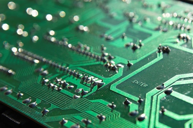
Printed Circuit Boards (PCBs) form the backbone of modern electronic devices, serving as the foundation upon which complex circuitry is built. The manufacturing process of PCB boards is a sophisticated and meticulous endeavor that requires precision, expertise, and advanced technology. This article delves into the complexities of PCB boards manufacturing, exploring the various stages involved, the technologies used, and the significance of quality control in ensuring the production of reliable and high-performance PCBs.
Understanding the Basics of PCBs
PCBs are designed to mechanically support and electrically connect electronic components using conductive pathways, tracks, or signal traces etched from copper sheets laminated onto a non-conductive substrate. The complexity of a PCB can range from a simple single-layer board to multi-layer boards with multiple layers of copper and insulating material. These boards are integral to the functionality of a vast array of electronic devices, from consumer electronics like smartphones and computers to industrial machinery and medical equipment.
The PCB Manufacturing Process
The manufacturing of PCB boards (https://conclusive.tech/services/pcb-design/) involves several key stages, each of which requires precision and attention to detail to ensure the final product meets the required specifications. The process begins with the design phase, where engineers use specialized software to create detailed schematics and layout designs for the PCB. These designs are then translated into a series of instructions that guide the manufacturing process.
One of the first steps in manufacturing is the creation of the substrate, typically made from fiberglass-reinforced epoxy resin known as FR4. This material provides the necessary strength and insulation properties for the PCB. Copper is then laminated onto the substrate to form the base layer for the conductive pathways. The copper-clad substrate undergoes a process called photoresist application, where a photosensitive material is applied to the surface.
The next stage involves the use of a photolithography process to transfer the PCB design onto the copper layer. A photographic film of the PCB layout is placed over the photoresist-coated substrate and exposed to ultraviolet light. The areas of the photoresist exposed to light harden, while the unexposed areas remain soft and can be removed. This step creates a precise pattern of the PCB traces on the copper layer.
Following the photolithography process, the PCB undergoes etching, where the unprotected copper is removed using a chemical solution, leaving behind the desired copper traces. The remaining photoresist is then stripped away, revealing the clean copper pathways. For multi-layer PCBs, this process is repeated for each layer, with additional steps for aligning and bonding the layers together.
Drilling and Plating
After the etching process, the PCB requires drilling to create holes for component leads and vias, which are conductive pathways that connect different layers of the board. High-precision drilling machines, often guided by computer numerical control (CNC) systems, are used to ensure accurate hole placement and sizing.
Once the holes are drilled, the PCB undergoes a plating process to deposit a thin layer of copper inside the holes, creating electrical connections between the layers. This is followed by a series of electroplating steps to build up the thickness of the copper traces and improve conductivity. The board may also undergo a process called solder masking, where a protective layer of solder mask is applied to prevent solder from bridging between conductors and causing short circuits.
Surface Finishing
Surface finishing is a critical step in PCB manufacturing, as it prepares the board for component assembly by enhancing solderability and protecting the exposed copper from oxidation. Several surface finish options are available, each with its advantages and applications. Common finishes include Hot Air Solder Leveling (HASL), Electroless Nickel Immersion Gold (ENIG), and Organic Solderability Preservative (OSP).
HASL involves coating the board with a layer of solder and then removing the excess using hot air, resulting in a smooth, solderable surface. ENIG provides a flat, gold-plated surface with excellent solderability and long shelf life, making it suitable for high-reliability applications. OSP, on the other hand, is a cost-effective, environmentally friendly finish that protects the copper surface until soldering.
Quality Control and Testing
Quality control is paramount in PCB manufacturing to ensure that the final product meets stringent performance and reliability standards. Throughout the manufacturing process, various inspection and testing methods are employed to detect and rectify defects. Automated Optical Inspection (AOI) systems use cameras and image processing software to examine the PCB for issues such as misaligned traces, shorts, and opens.
Electrical testing, including Flying Probe Testing and In-Circuit Testing (ICT), is conducted to verify the electrical integrity of the PCB. These tests check for continuity, insulation resistance, and proper functioning of the circuitry. Additional tests, such as X-ray inspection and thermal cycling, may be performed to assess the board’s structural integrity and performance under different conditions.
The Role of Advanced Technologies
The manufacturing of PCB boards has evolved significantly with the advent of advanced technologies. Automation plays a crucial role in enhancing precision, efficiency, and scalability in PCB production. Automated machinery for drilling, plating, and inspection reduces human error and increases throughput, enabling the production of high-quality PCBs in large volumes.
The use of computer-aided design (CAD) and computer-aided manufacturing (CAM) software streamlines the design and production process, allowing for the rapid prototyping and iteration of PCB designs. These tools enable engineers to optimize layouts, simulate performance, and identify potential issues before manufacturing, reducing time-to-market and development costs.
Moreover, advancements in materials science have led to the development of high-performance substrates and conductive materials that improve the electrical and thermal properties of PCBs. Innovations such as flexible PCBs, which can be bent and shaped to fit unique form factors, have expanded the applications of PCBs in wearable technology, medical devices, and aerospace.
Sustainability in PCB Manufacturing
As environmental concerns become increasingly important, the PCB manufacturing industry is adopting more sustainable practices. Efforts to reduce the environmental impact of PCB production include minimizing waste, recycling materials, and using eco-friendly chemicals and processes. Lead-free soldering, for instance, eliminates the use of toxic lead in solder, reducing the environmental and health hazards associated with PCB manufacturing.
Additionally, manufacturers are exploring the use of biodegradable substrates and conductive inks made from organic materials. These innovations aim to reduce the environmental footprint of electronic devices and promote the development of greener technologies.
The Future of PCB Manufacturing
The future of PCB manufacturing is poised to be shaped by ongoing technological advancements and the growing demand for more complex and miniaturized electronic devices. The integration of emerging technologies such as the Internet of Things (IoT), artificial intelligence (AI), and 5G connectivity will drive the need for more sophisticated PCBs with enhanced capabilities.
The development of advanced manufacturing techniques, such as additive manufacturing (3D printing), holds the potential to revolutionize PCB production by enabling the creation of highly customized and complex designs with reduced lead times and material waste. Furthermore, the continued push for sustainability will likely lead to more eco-friendly manufacturing processes and materials, aligning with global efforts to combat climate change and reduce electronic waste.
Conclusion
PCB boards manufacturing is a complex and multifaceted process that requires a combination of precision engineering, advanced technology, and rigorous quality control. From the initial design phase to the final testing and inspection, each step in the manufacturing process plays a crucial role in ensuring the production of reliable, high-performance PCBs. As technology continues to advance and the demand for sophisticated electronic devices grows, the PCB manufacturing industry will continue to evolve, driven by innovation, automation, and sustainability. By staying at the forefront of these developments, manufacturers can deliver cutting-edge solutions that meet the ever-changing needs of the global market – https://conclusive.tech


